Xilinx Vertex 5 FPGA
This project was completed for the UC Berkeley EECS150 (Components and Design Techniques for Digital Systems) class. It is a complete digital system design implementing a three-stage pipelined MIPS instruction set architecture (ISA) mapped onto a Xilinx Vertex 5 Reprogrammable FPGA using Verilog HDL.
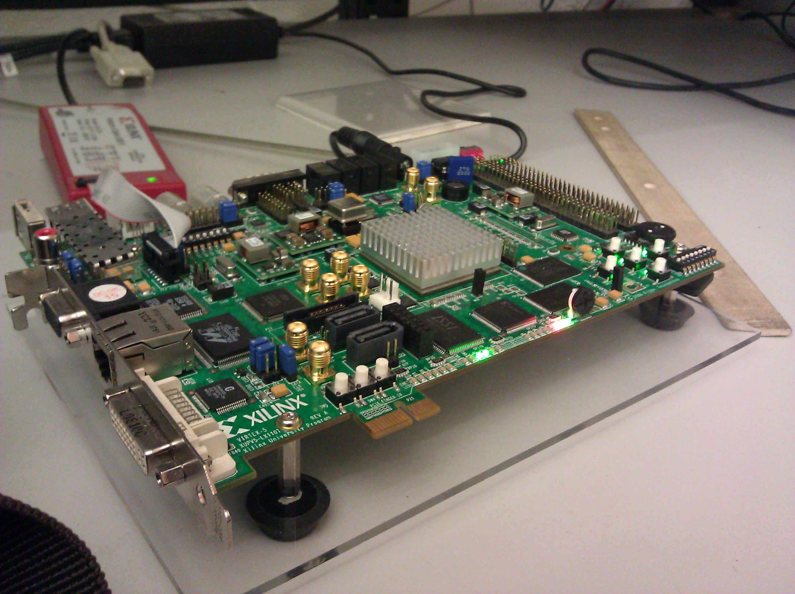 Figure 1. Xilinx FPGA development board in the Berkeley EECS Cory Lab.
This semester-long project involved designing everything from scratch, including memory structures (RAM/ROM), block-RAM controllers, the Arithmetic Logic Unit (ALU) for the execute stage, and control logic to resolve branch delay slots and pipeline hazards.
The core challenge of this project lay in the physical debugging. Unlike high-level sequential programming, writing code for hardware requires meticulous timing analysis, signal probing using logic analyzers, and thorough simulation to diagnose transient state errors.
Final Project Report
Read our complete structural report on the MIPS hardware implementation, pipeline architecture, and laboratory results.
View Final Report (PDF)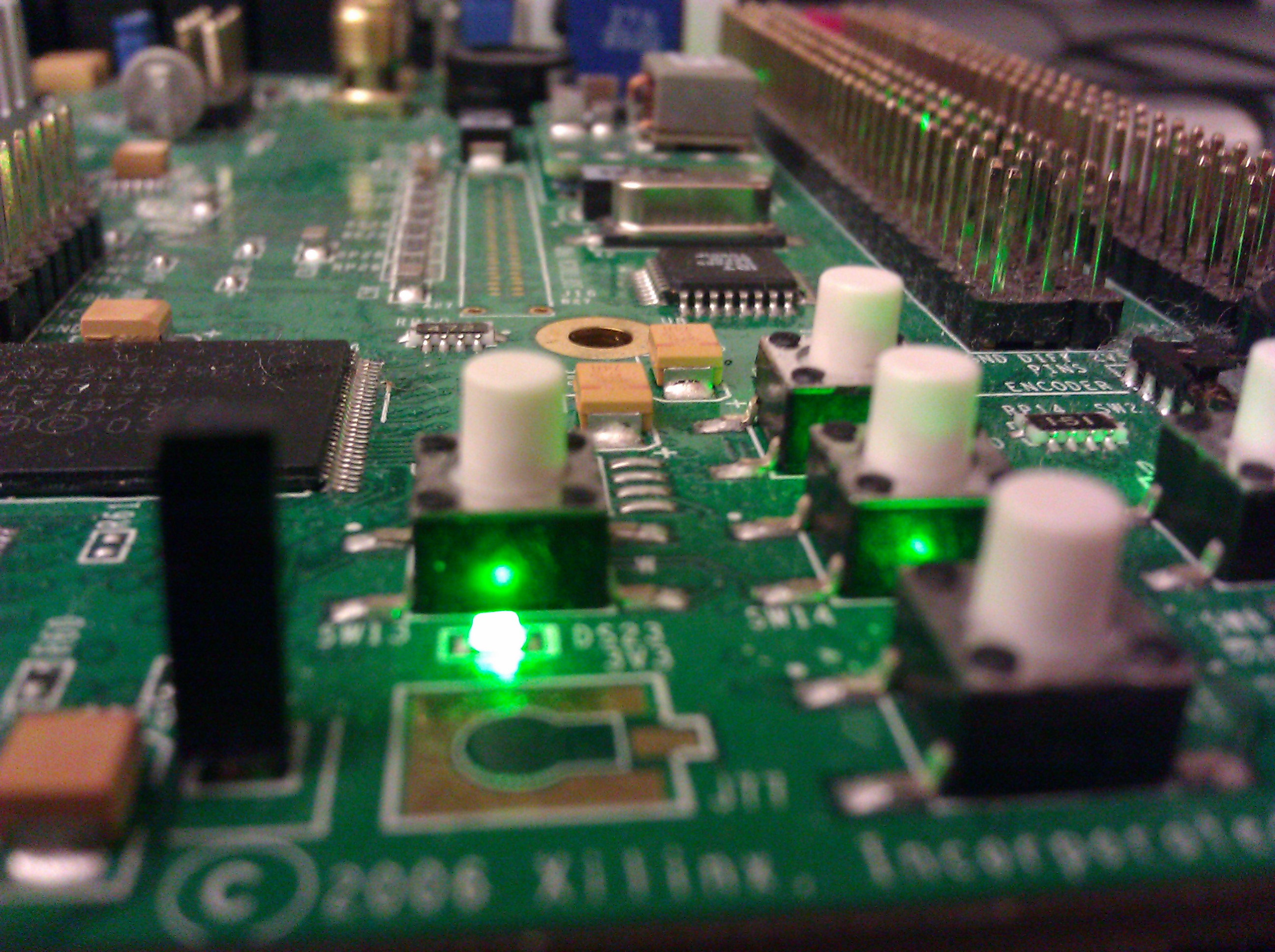 Figure 2. Closeup view of the Xilinx Vertex-5 FPGA silicon chip.
Project Specs
- Platform: Xilinx Vertex-5 FPGA
- Language: Verilog HDL
- Architecture: MIPS 3-Stage Pipeline
- Course: UC Berkeley EECS150
- Timeline: Semester Project (Fall 2011)